Learn bits
Science & Tech.
Mahesh

09/04/24 06:09 AM IST
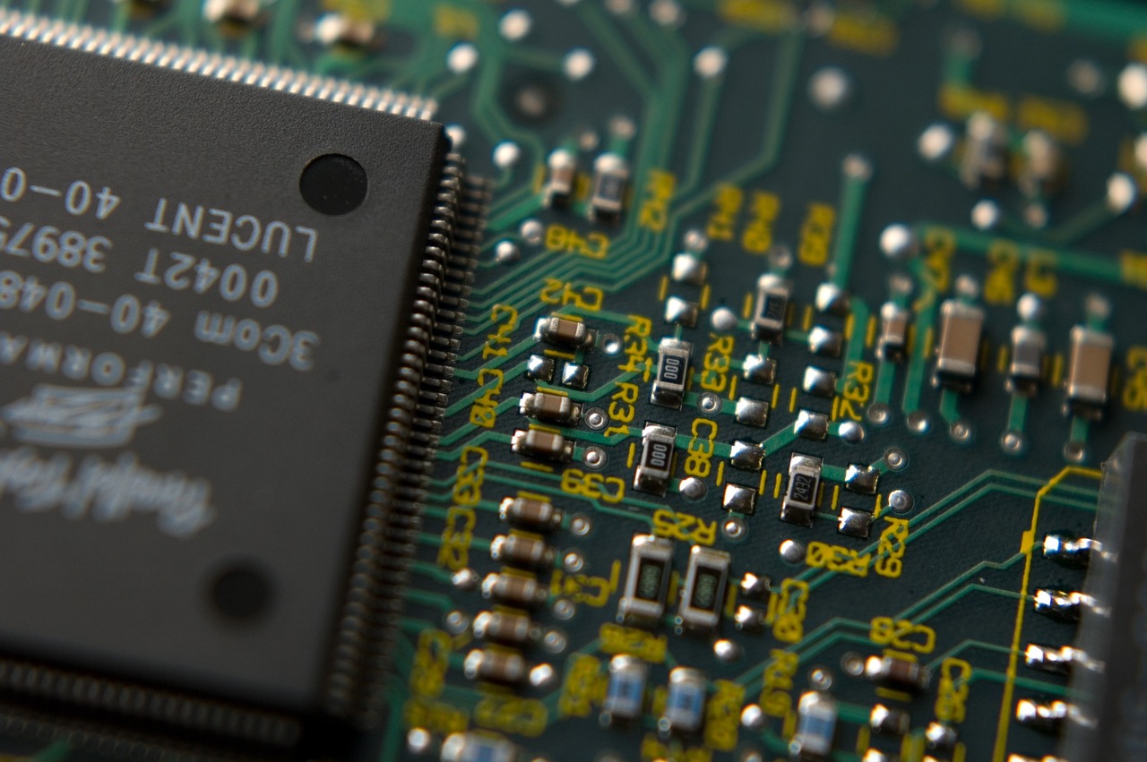
Semiconductor Chip

In News
  • The TATA group has partnered with Taiwan’s Powerchip Semiconductor Manufacturing Corporation (PSMC) to set-up a 300mm wafer fabrication plant in Gujarat.
  • It will roll out its first 28nm chip in 2026.
Semiconductor chip
  • A semiconductor has properties between a conductor (which conducts electricity) and an insulator (which does not).
  • In its purest form a semiconductor is a very weak conductor of electricity.
  • However, its electrical properties can be changed by adding small amounts of certain substances called ‘dopants’.
  • By taking a pure semiconductor and carefully injecting certain parts with specific dopants, complex circuits can be ‘printed’ on the semiconductor.
  • The process is crudely analogous to creating an intricate work of art on a paper or a wall, by using a bunch of stencils and spray paints of different colours.
  • The stencils are called ‘masks’ in the industry and the paint is analogous to the dopant.
Transistor
  • The transistor, one of the earliest electronic components to be built using a semiconductor, is an extremely versatile device. In its most popular form it can function as an electronic switch.
  • A typical semiconductor chip can have millions/billions of these interconnected switches that work together to perform various logical and computational operations.
  • A transistor can also function as an amplifier (to amplify the weak signal received by your cell phone) and is an integral part of circuits that generate and process high frequency signals (such as those required in wireless communication technologies).
  • Today all these different avatars of the transistor are routinely packed into a single semiconductor chip (such as the WiFi chip in your mobile).
  • The transistor demonstrated how a single device could be built out of a piece of a semiconductor.
  • Printing’ multiple devices onto a single piece of a semiconductor to create entire circuits was the next leap.
  • Both these breakthroughs laid the foundation for the semiconductor revolution and have been aptly recognised by Nobel Prizes (in 1956 and 2000).
Fabrication Technology
  • Technology has progressed at a relentless pace since the semiconductor chip was first conceptualised more than six decades ago.
  • Newer manufacturing technologies have been introduced at a regular cadence.
  • The level of miniaturisation of the semiconductor has increased by orders of magnitude.
  • Sticking with the stencil analogy this is mainly due to the stencils being able to etch smaller and more intricate patterns.
  • There have been equally impressive gains in the switching capability of the transistors.
  • They are able to switch on-and-off faster (more computations per second) and with lesser power consumption (longer battery life and lesser heat dissipation).
  • The industry has used labels like ‘45nm’, ‘28nm’ and ‘16nm’ to introduce each new manufacturing technology. ‘nm’ is short for nano-meter and refers to an extremely small unit of length equal to one billionth of a meter.
  • These numbers convey the level of miniaturisation that is achievable using a particular technology (so smaller is better).
  • Though not always accurate, you can think of this number as representing the dimensions of single transistor.
  • While traditionally electronic circuits have been laid out flat on the semiconductor, researchers are increasing looking to capitalise on the third dimension (height).
  • As the length and breadth of a transistor switch decreases, increasing its height can help ensure reliable performance.
  • Stacking entire circuits on top of one another is another way to continue to shrink semiconductor chip sizes.
About Wafer
  • A semiconductor chip is manufactured much like a postage stamp. A sheet of stamps is printed on a piece of paper and then each individual stamp is cut out.
  • Similarly, an array (typically 300-400) of chips are printed on a circular piece of semiconductor (called a wafer in industry parlance).
  • This is then diced to create individual chips. A larger wafer size allows more chips to be printed on a single wafer which makes chip production faster and cheaper.
  • Wafer sizes used in the industry have constantly been increasing.
  • The current state of art is 300mm which is approximately 12 inches (this refers to the diameter of the wafer).
  • Efforts are ongoing to move to a 450mm wafer size. While moving to a larger wafer size has its technical challenges and capital expenses, it has proven to be economical in the long run.
  • Once the wafer has been diced into chips, each individual chip has to be packaged in a protective covering.
  • Tiny wires have to be routed from the device to the boundary of the package.
  • Some of these wires supply power, while other are used for feeding in and reading out signals and data.
  • A chip also has to be tested — this includes verifying its functionality and stress testing (subjecting the chip to high temperature and voltages) — to ensure reliability during its lifetime. All this is performed in an assembly and test plant.
India's Semiconductor Ecosystem
  • India has had a thriving chip design industry since the 1990s.
  • Due to the magic of computer aided design it is possible to design a semiconductor chip entirely in software.
  • The process of specifying the functionality of a chip, translating this functionality to electronic circuits, validating the circuits, optimising for speed, power consumption and size, can be done by a team of skilled engineers sitting at their desktops.
  • The final design is abstracted into a file and sent to a fabrication plant for manufacturing. It’s a bit like designing an entire graphic novel on your laptop and then sending the pdf to your publisher for printing.
  • India’s foray into semiconductor manufacturing will benefit from the existing ecosystem for chip design which was fuelled by a steady supply of electronics and computer engineers.
  • Semiconductor manufacturing being an essentially inter-disciplinary endeavour, could present opportunities to a wider array of professionals such as process and control engineers, data scientists, material scientists, physicists and chemical engineers to contribute meaningfully to this industry.
Source- The Hindu

More Related Current Affairs View All

10 Jan

Rural landowners in Delhi want repeal of Sections 33 and 81 of Delhi Land Reforms Act

'Both sections dealing with the use and sale of agricultural land have come under the spotlight ahead of the Delhi Assembly elections.' This can only be done by the Central gove

Read More

10 Jan

Pravasi Bharatiya Diwas

'Prime Minister Narendra Modi inaugurated the 18th edition of the Pravasi Bharatiya Diwas  in Bhubaneswar.' The event is held once every two years to “honour the cont

Read More

10 Jan

Deciphering the Indus script

'Recently, Tamil Nadu Chief Minister M.K. Stalin announced a $1-million prize for experts or organisations in the event of their success in deciphering the scripts of the Indus Val

Read More

India’s First Ai-Driven Magazine Generator

Generate Your Custom Current Affairs Magazine using our AI in just 3 steps